(Information taken from Data Sheet dated October 1982)
Features
| Supply voltage range | VCC | 9.5 to 18 V | |||
| Supply current, unloaded | ICC | typ. | 4.5 mA | ||
| Input voltage, all inputs | |||||
|
VIH | min. | 7.5 V | ||
|
VIL | max. | 4.5 V | ||
| Input current, all inputs, LOW | IIL | typ. | 30 µA | ||
| Output current LOW | IOL | max. | 500 mA | ||
| Operating ambient temperature range | Tamb | -20 to +70 °C | |||
Package outline - 16-lead DIL; plastic (SOT-38A)
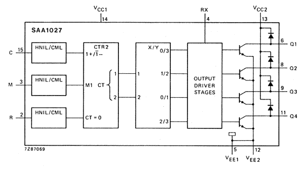
Fig. 1 Block diagram. The blocks marked HNIL/CML are high noise immunity input stages, the block marked CTR2 is a bidirectional sychronous 2-bit (4-state) counter and the block marked X/Y is a code converter. C is the count input, M the mode input to select forward or reverse counting and R is the reset input which resets the counter to content zero.
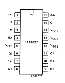
| 1 | n.c. | not connected |
| 2 | R | reset input |
| 3 | M | mode input |
| 4 | RX | external resistor |
| 5 | VEE1 | ground |
| 6 | Q1 | output 1 |
| 7 | n.c. | not connected |
| 8 | Q2 | output 2 |
| 9 | Q3 | output 3 |
| 10 | n.c. | not connected |
| 11 | Q4 | output 4 |
| 12 | VEE2 | ground |
| 13 | VCC2 | positive supply |
| 14 | VCC1 | positive supply |
| 15 | C | count input |
| 16 | n.c. | not connected |
Mode input M (pin 3)
With the mode input the sequence of output signals, and hence the direction of the stepping motor,
can be chosen, as shown in the following table.
| Counting sequence |
M = L | M = H | ||||||
| Q1 | Q2 | Q3 | Q4 | Q1 | Q2 | Q3 | Q4 | |
| 0 | L | H | L | H | L | H | L | H |
| 1 | H | L | L | H | L | H | H | L |
| 2 | H | L | H | L | H | L | H | L |
| 3 | L | H | H | L | H | L | L | H |
| 0 | L | H | L | H | L | H | L | H |
Reset input (pin 2)
A LOW level at the R input resets the counter to zero. The outputs take on the levels shown in
the upper and lower line of the table above.
If this facility is not used the R input should be connected to the supply.
External resistor pin RX (pin 4)
The External resistor pin R4 connected to RX sets the base current of the output transistors.
Its value has to be chosen in accordance with the required output current (see Fig. 5).
Outputs Q1 to Q4 (pins 6, 8, 9, and 11)
The circuit has open-collector outputs. To prevent damage by an overshooting output voltage
the outputs are protected by diodes connected to VCC2, pin 13.
High output currents mainly determine the total power dissipation, see Fig. 3.
| Supply voltage, d.c. | VCC1;VCC2 | max. | 18 V |
| Input voltage, all inputs | VI | max. | 18 V |
| Current into pin 4 | IRX | max. | 120 mA |
| Output current | IOL | max. | 500 mA |
| Power dissipation | Ptot | see Fig.4 | |
| Storage temperature range | Tstg | -40 to +125 °C | |
| Operating ambient temperature range | Tamb | -20 to +70 °C | |
| parameter | symbol | min. | typ. | max. | unit |
| Supply VCC1 and VCC2 (pins 14 and 13) Supply Current at VCC1 = 12 V; unloaded; all inputs HIGH; pin 4 open |
ICC | 2 | 4.5 | 6.5 | mA |
| Inputs C, M and R (pins 15, 3 and 2) Input voltage: HIGH LOW Input current: HIGH LOW |
VIH VIL IIH -IIL |
7.5 - - - | - - 1 30 | - 4.5 - - | V V µA µA |
| External resistor pin RX (pin 4) Voltage at RX at VCC = 12 V ± 15% R4 = 130 ohm ± 5% |
VRX | 3 | - | 4.5 | V |
| Outputs Q1 to Q4 Output voltage LOW at IOL = 350 mA at IOL = 500 mA Output current LOW HIGH at VQ = 18 V | VOL VOL IOL -IOH |
- - - - |
500 700 - - |
1000 - 500* 50 |
mV mV mA µA |
* See figs 3 and 4
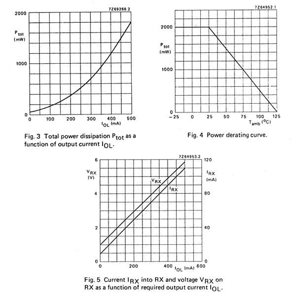
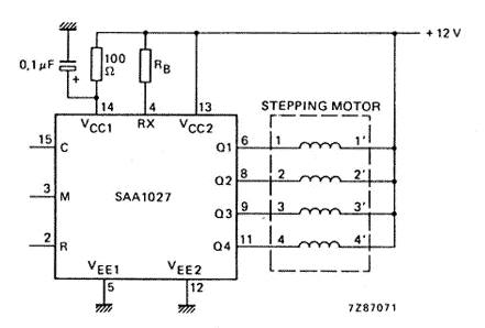
Fig.6 Typical application of the SAA1027 as a stepping motor driver.